- 您现在的位置:买卖IC网 > Sheet目录3891 > PIC18C801T-I/L (Microchip Technology)IC MCU ROMLESS A/D PWM 84PLCC
PIC18C601/801
DS39541A-page 128
Advance Information
2001 Microchip Technology Inc.
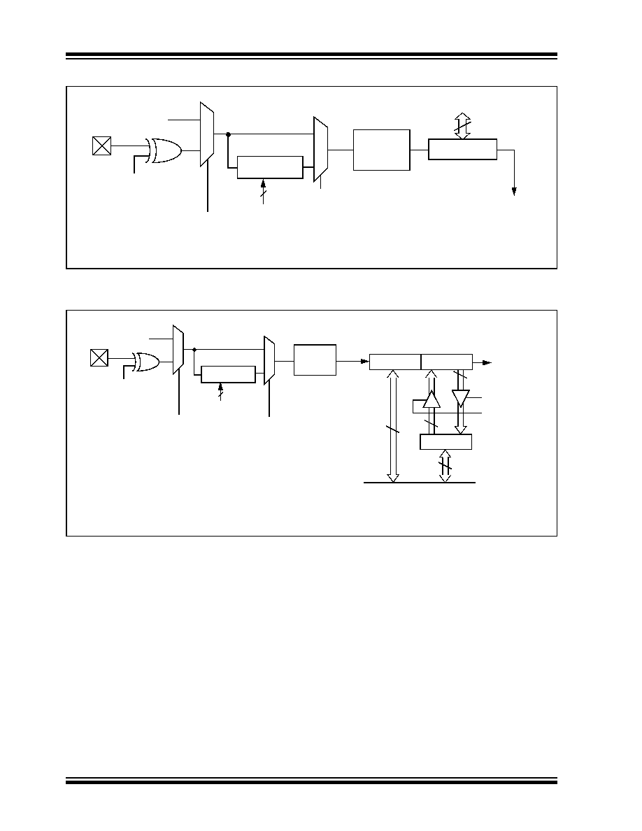
FIGURE 10-1:
TIMER0 BLOCK DIAGRAM IN 8-BIT MODE
FIGURE 10-2:
TIMER0 BLOCK DIAGRAM IN 16-BIT MODE
Note 1: Upon RESET, Timer0 is enabled in 8-bit mode with clock input from T0CKI max. prescale.
2: I/O pins have diode protection to VDD and VSS.
RA4/T0CKI
T0SE
0
1
0
1
pin(2)
T0CS(1)
FOSC/4
Programmable
Prescaler
Sync with
Internal
Clocks
TMR0L
(2 TCY delay)
Data Bus
8
PSA
T0PS2, T0PS1, T0PS0
Set Interrupt
Flag bit TMR0IF
on Overflow
3
RA4/T0CKI
T0SE
0
1
0
1
T0CS(1)
FOSC/4
Programmable
Prescaler
Sync with
Internal
Clocks
TMR0L
(2 TCY delay)
Data Bus<7:0>
8
PSA
T0PS2, T0PS1, T0PS0
Set Interrupt
Flag bit TMR0IF
on Overflow
3
TMR0
TMR0H
High Byte
8
Read TMR0L
Write TMR0L
Note 1: Upon RESET, Timer0 is enabled in 8-bit mode with clock input from T0CKI max. prescale.
2: I/O pins have diode protection to VDD and VSS.
pin(2)
发布紧急采购,3分钟左右您将得到回复。
相关PDF资料
PIC18C658T-I/L
IC MCU OTP 16KX16 CAN 68PLCC
PIC18C658T-E/L
IC MCU OTP 16KX16 CAN 68PLCC
PIC16C925T-I/L
IC MCU OTP 4KX14 LCD DVR 68PLCC
PIC12F675-E/P
IC MCU CMOS 1K FLASH W/AD 8-DIP
PIC18C858T-E/L
IC MCU OTP 16KX16 CAN 84PLCC
PIC16F636-I/SL
IC PIC MCU FLASH 2KX14 14-SOIC
PIC18LC658T-I/L
IC MCU OTP 16KX16 CAN 68PLCC
PIC18LC801T-I/L
IC MCU ROMLESS A/D PWM 84PLCC
相关代理商/技术参数
PIC18C801T-I/PT
功能描述:8位微控制器 -MCU 2MB 1536 RAM 37I/O RoHS:否 制造商:Silicon Labs 核心:8051 处理器系列:C8051F39x 数据总线宽度:8 bit 最大时钟频率:50 MHz 程序存储器大小:16 KB 数据 RAM 大小:1 KB 片上 ADC:Yes 工作电源电压:1.8 V to 3.6 V 工作温度范围:- 40 C to + 105 C 封装 / 箱体:QFN-20 安装风格:SMD/SMT
PIC18C858-E/L
功能描述:8位微控制器 -MCU 32KB 1536 RAM 68I/O RoHS:否 制造商:Silicon Labs 核心:8051 处理器系列:C8051F39x 数据总线宽度:8 bit 最大时钟频率:50 MHz 程序存储器大小:16 KB 数据 RAM 大小:1 KB 片上 ADC:Yes 工作电源电压:1.8 V to 3.6 V 工作温度范围:- 40 C to + 105 C 封装 / 箱体:QFN-20 安装风格:SMD/SMT
PIC18C858-E/PT
功能描述:8位微控制器 -MCU 32KB 1536 RAM 68I/O RoHS:否 制造商:Silicon Labs 核心:8051 处理器系列:C8051F39x 数据总线宽度:8 bit 最大时钟频率:50 MHz 程序存储器大小:16 KB 数据 RAM 大小:1 KB 片上 ADC:Yes 工作电源电压:1.8 V to 3.6 V 工作温度范围:- 40 C to + 105 C 封装 / 箱体:QFN-20 安装风格:SMD/SMT
PIC18C858EPT
制造商:MICRO CHIP 功能描述:New
PIC18C858-I/L
功能描述:8位微控制器 -MCU 32KB 1536 RAM 68I/O RoHS:否 制造商:Silicon Labs 核心:8051 处理器系列:C8051F39x 数据总线宽度:8 bit 最大时钟频率:50 MHz 程序存储器大小:16 KB 数据 RAM 大小:1 KB 片上 ADC:Yes 工作电源电压:1.8 V to 3.6 V 工作温度范围:- 40 C to + 105 C 封装 / 箱体:QFN-20 安装风格:SMD/SMT
PIC18C858-I/PT
功能描述:8位微控制器 -MCU 32KB 1536 RAM 68I/O RoHS:否 制造商:Silicon Labs 核心:8051 处理器系列:C8051F39x 数据总线宽度:8 bit 最大时钟频率:50 MHz 程序存储器大小:16 KB 数据 RAM 大小:1 KB 片上 ADC:Yes 工作电源电压:1.8 V to 3.6 V 工作温度范围:- 40 C to + 105 C 封装 / 箱体:QFN-20 安装风格:SMD/SMT
PIC18C858T-E/L
功能描述:8位微控制器 -MCU 40MHz 16K OTP RoHS:否 制造商:Silicon Labs 核心:8051 处理器系列:C8051F39x 数据总线宽度:8 bit 最大时钟频率:50 MHz 程序存储器大小:16 KB 数据 RAM 大小:1 KB 片上 ADC:Yes 工作电源电压:1.8 V to 3.6 V 工作温度范围:- 40 C to + 105 C 封装 / 箱体:QFN-20 安装风格:SMD/SMT
PIC18C858T-E/PT
功能描述:8位微控制器 -MCU 32KB 1536 RAM 68I/O RoHS:否 制造商:Silicon Labs 核心:8051 处理器系列:C8051F39x 数据总线宽度:8 bit 最大时钟频率:50 MHz 程序存储器大小:16 KB 数据 RAM 大小:1 KB 片上 ADC:Yes 工作电源电压:1.8 V to 3.6 V 工作温度范围:- 40 C to + 105 C 封装 / 箱体:QFN-20 安装风格:SMD/SMT